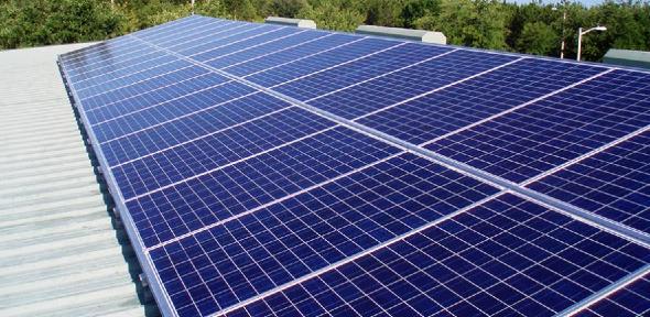
A team of researchers from the UK and Japan has found that the tiny defects which limit the efficiency of perovskites – cheaper alternative materials for solar cells – are also responsible for structural changes in the material that lead to degradation.
The multi-disciplinary team of researchers used a combination of techniques to mimic the process of aging under sunlight and observe changes in the materials at the nanoscale, helping them gain new insights into the materials, which also show potential for optoelectronic applications such as energy-efficient LEDs and X-ray detectors, but are limited in their longevity. Their results could significantly accelerate the development of long-lasting, commercially available perovskite photovoltaics.
"Perovskites offer a viable option for low- and middle-income countries looking to transition to solar energy, ” Dr Stuart MacPherson, Cavendish Laboratory, University of Cambridge
Perovksites are abundant and much cheaper to process than crystalline silicon. They can be prepared in liquid ink that is simply printed to produce a thin film of the material. While the overall energy output of perovskite solar cells can often meet or – in the case of multi-layered ‘tandem’ devices – exceed that achievable with traditional silicon photovoltaics, the limited longevity of the devices is a key barrier to their commercial viability.
A typical silicon solar panel, like those you might see on the roof of a house, typically lasts about 20-25 years without significant performance losses. Because perovskite devices are much cheaper to produce, they may not need to have as long a lifetime as their silicon counterparts to enter some markets. But to fulfill their ultimate potential in realising widespread decarbonisation, cells will need to operate for at least a decade or more. Researchers and manufacturers have yet to develop a perovskite device with similar stability to silicon cells.
Now, researchers at the University of Cambridge and the Okinawa Institute of Science and Technology (OIST) in Japan, have discovered the secret to treating the ‘Achilles heel’ of perovskites. Using high spatial-resolution techniques, in collaboration with the Diamond Light Source synchrotron facility and its electron Physical Sciences Imaging Centre (ePSIC) in Oxfordshire, and the Department of Materials Science and Metallurgy in Cambridge, the team was able to observe the nanoscale properties of these thin films and how they change over time under solar illumination.
Previous work by the team using similar techniques has shone light on the defects that cause deficiencies in the performance of perovskite photovoltaics – so-called carrier traps.
"It’s pretty exciting, because it suggests that if you can address the formation of these surface traps, then you will simultaneously improve performance and the stability of the devices over time. ” Dr Tiarnan Doherty, Department of Chemical Engineering and Biotechnology, University of Cambridge
"We now understand that any residual unwanted phases – even tiny nanoscale pockets remaining from the processing of the cells – will be bad news for the longevity of perovskite solar cells. The manufacturing processes need to incorporate careful tuning of the structure and composition across a large area to eliminate any trace of these unwanted phases – even more careful control than is widely thought for these materials. This is a great example of fundamental science directly guiding scaled manufacturing.” Dr Sam Stranks, Cavendish Laboratory, University of Cambridge
Read the full University of Cambridge article here.
Image credit: Alachua County

